Friday 25 September 2009

Noise and Electrical Distortion

Because of the very high switching rate and relatively low signal strength found on data, address, and other buses within a computer, direct extension of the buses beyond the confines of the main circuit board or plug-in boards would pose serious problems. First, long runs of electrical conductors, either on printed circuit boards or through cables, act like receiving antennas for electrical noise radiated by motors, switches, and electronic circuits:


Such noise becomes progressively worse as the length increases, and may eventually impose an unacceptable error rate on the bus signals. Just a single bit error in transferring an instruction code from memory to a microprocessor chip may cause an invalid instruction to be introduced into the instruction stream, in turn causing the computer to totally cease operation.
A second problem involves the distortion of electrical signals as they pass through metallic conductors. Signals that start at the source as clean, rectangular pulses may be received as rounded pulses with ringing at the rising and falling edges:

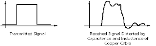
These effects are properties of transmission through metallic conductors, and become more pronounced as the conductor length increases. To compensate for distortion, signal power must be increased or the transmission rate decreased.
Special amplifier circuits are designed for transmitting direct (unmodulated) digital signals through cables. For the relatively short distances between components on a printed circuit board or along a computer backplane, the amplifiers are in simple IC chips that operate from standard +5v power. The normal output voltage from the amplifier for logic '1' is slightly higher than the minimum needed to pass the logic '1' threshold. Correspondingly for logic '0', it is slightly lower. The difference between the actual output voltage and the threshold value is referred to as the noise margin, and represents the amount of noise voltage that can be added to the signal without creating an error:


Asynchronous vs. Synchronous Transmission

Serialized data is not generally sent at a uniform rate through a channel. Instead, there is usually a burst of regularly spaced binary data bits followed by a pause, after which the data flow resumes. Packets of binary data are sent in this manner, possibly with variable-length pauses between packets, until the message has been fully transmitted. In order for the receiving end to know the proper moment to read individual binary bits from the channel, it must know exactly when a packet begins and how much time elapses between bits. When this timing information is known, the receiver is said to be synchronized with the transmitter, and accurate data transfer becomes possible. Failure to remain synchronized throughout a transmission will cause data to be corrupted or lost.
Two basic techniques are employed to ensure correct synchronization. In synchronous systems, separate channels are used to transmit data and timing information. The timing channel transmits clock pulses to the receiver. Upon receipt of a clock pulse, the receiver reads the data channel and latches the bit value found on the channel at that moment. The data channel is not read again until the next clock pulse arrives. Because the transmitter originates both the data and the timing pulses, the receiver will read the data channel only when told to do so by the transmitter (via the clock pulse), and synchronization is guaranteed.

Techniques exist to merge the timing signal with the data so that only a single channel is required. This is especially useful when synchronous transmissions are to be sent through a modem. Two methods in which a data signal is self-timed are nonreturn-to-zero and biphase Manchester coding. These both refer to methods for encoding a data stream into an electrical waveform for transmission.In asynchronous systems, a separate timing channel is not used. The transmitter and receiver must be preset in advance to an agreed-upon baud rate. A very accurate local oscillator within the receiver will then generate an internal clock signal that is equal to the transmitter's within a fraction of a percent. For the most common serial protocol, data is sent in small packets of 10 or 11 bits, eight of which constitute message information. When the channel is idle, the signal voltage corresponds to a continuous logic '1'. A data packet always begins with a logic '0' (the start bit) to signal the receiver that a transmission is starting. The start bit triggers an internal timer in the receiver that generates the needed clock pulses. Following the start bit, eight bits of message data are sent bit by bit at the agreed upon baud rate. The packet is concluded with a parity bit and stop bit. One complete packet is illustrated below:


Data Encryption.Privacy is a great concern in data communications. Faxed business letters can be intercepted at will through tapped phone lines or intercepted microwave transmissions without the knowledge of the sender or receiver. To increase the security of this and other data communications, including digitized telephone conversations, the binary codes representing data may be scrambled in such a way that unauthorized interception will produce an indecipherable sequence of characters. Authorized receive stations will be equipped with a decoder that enables the message to be restored. The process of scrambling, transmitting, and descrambling is known as encryption.
Custom integrated circuits have been designed to perform this task and are available at low cost. In some cases, they will be incorporated into the main circuitry of a data communications device and function without operator knowledge. In other cases, an external circuit is used so that the device, and its encrypting/decrypting technique, may be transported easily.


What is Data Communications?

The distance over which data moves within a computer may vary from a few thousandths of an inch, as is the case within a single IC chip, to as much as several feet along the backplane of the main circuit board. Over such small distances, digital data may be transmitted as direct, two-level electrical signals over simple copper conductors. Except for the fastest computers, circuit designers are not very concerned about the shape of the conductor or the analog characteristics of signal transmission.
Frequently, however, data must be sent beyond the local circuitry that constitutes a computer. In many cases, the distances involved may be enormous. Unfortunately, as the distance between the source of a message and its destination increases, accurate transmission becomes increasingly difficult. This results from the electrical distortion of signals traveling through long conductors, and from noise added to the signal as it propagates through a transmission medium. Although some precautions must be taken for data exchange within a computer, the biggest problems occur when data is transferred to devices outside the computer's circuitry. In this case, distortion and noise can become so severe that information is lost.
Data Communications concerns the transmission of digital messages to devices external to the message source. "External" devices are generally thought of as being independently powered circuitry that exists beyond the chassis of a computer or other digital message source. As a rule, the maximum permissible transmission rate of a message is directly proportional to signal power, and inversely proportional to channel noise. It is the aim of any communications system to provide the highest possible transmission rate at the lowest possible power and with the least possible noise

Communications Channels A communications channel is a pathway over which information can be conveyed. It may be defined by a physical wire that connects communicating devices, or by a radio, laser, or other radiated energy source that has no obvious physical presence. Information sent through a communications channel has a source from which the information originates, and a destination to which the information is delivered. Although information originates from a single source, there may be more than one destination, depending upon how many receive stations are linked to the channel and how much energy the transmitted signal possesses.
In a digital communications channel, the information is represented by individual data bits, which may be encapsulated into multibit message units. A byte, which consists of eight bits, is an example of a message unit that may be conveyed through a digital communications channel. A collection of bytes may itself be grouped into a frame or other higher-level message unit. Such multiple levels of encapsulation facilitate the handling of messages in a complex data communications network.


The message source is the transmitter, and the destination is the receiver. A channel whose direction of transmission is unchanging is referred to as a simplex channel. For example, a radio station is a simplex channel because it always transmits the signal to its listeners and never allows them to transmit back.
A half-duplex channel is a single physical channel in which the direction may be reversed. Messages may flow in two directions, but never at the same time, in a half-duplex system. In a telephone call, one party speaks while the other listens. After a pause, the other party speaks and the first party listens. Speaking simultaneously results in garbled sound that cannot be understood.
A full-duplex channel allows simultaneous message exchange in both directions. It really consists of two simplex channels, a forward channel and a reverse channel, linking the same points. The transmission rate of the reverse channel may be slower if it is used only for flow control of the forward channel.

Serial Communications.Most digital messages are vastly longer than just a few bits. Because it is neither practical nor economic to transfer all bits of a long message simultaneously, the message is broken into smaller parts and transmitted sequentially. Bit-serial transmission conveys a message one bit at a time through a channel. Each bit represents a part of the message. The individual bits are then reassembled at the destination to compose the message. In general, one channel will pass only one bit at a time. Thus, bit-serial transmission is necessary in data communications if only a single channel is available. Bit-serial transmission is normally just called serial transmission and is the chosen communications method in many computer peripherals.
Byte-serial transmission conveys eight bits at a time through eight parallel channels. Although the raw transfer rate is eight times faster than in bit-serial transmission, eight channels are needed, and the cost may be as much as eight times higher to transmit the message. When distances are short, it may nonetheless be both feasible and economic to use parallel channels in return for high data rates. The popular Centronics printer interface is a case where byte-serial transmission is used. As another example, it is common practice to use a 16-bit-wide data bus to transfer data between a microprocessor and memory chips; this provides the equivalent of 16 parallel channels. On the other hand, when communicating with a timesharing system over a modem, only a single channel is available, and bit-serial transmission is required. This figure illustrates these ideas:


Wednesday 2 September 2009

Wireless Network

Wireless network pass on to any kind of computer network that is cable less and generally linked with a telecommunications and based on IEEE 802.11. Wireless Network can implement between nodes without any wire and remote information transmission system uses the radio waves, at the physical level of the network. There are several benefits of Wireless Network such as file sharing, Internet connection sharing, multi-player games, Internet telephone service, Computer mobility, and No unsightly wires. 802.11 support networking bandwidth and have an array of choices such as 802.11b, 802.11a,802.11g, 802.11n also known as Wi-Fi technologies and designed for precise networking programs. The hardware requirements of a Wireless network are Network adapter, Repeater, Network hub, and Modem.
There are different types of Wireless Networks such as LAN in which radio signals are used instead of wires and transmit data from one Pc to other Pc in the same network as it is Wi-Fi is a wireless network that enables connection to internet with WiFi functionality. it produced radio waves that can be picked up by WiFi receiver and fixed wireless data is also type of LAN that can be connect more then one building with the mean of sharing .The MAN have ability to connect several local area networks and a term WiMax used to represent wireless metropolitan area networks and Mobile devices networks contains Global System for Mobile Communications which is called GSM network and mainly used for cellular phones, Personal Communications Service is a radio band used to set up PCS and D-AMPS is an upgrade version of AMPS.
A Wireless network containing basic setup and to use a wireless network you have to need a networking card and Kernel config require IEEE 802.11 wireless network driver, Hardware Access Layer and ample Rate control algorithm. Wireless to crypto support modules .There are different kind of protocol used in a Wireless network, it has routing protocol such as DSDV, AODV, B.A.T.M.A.N, PWRP, DSR, OLSR, OORP, TORA,HSLS and The Ad-Hoc Configuration Protocol and Proactive Auto configuration. There are different related terms used for wireless network like WEP is a security protocol from IEEE, SSID, Static IP, DHCP, Subnet, LAN, WLAN, MAC, WAP, and Sniffer but the most commonly used term in these days is Wi-Fi such a technology wrapping the world.
Wireless network faces much security threat due to some reason as Spread spectrum used in LAN not very protected because the spreading codes openly therefore companies can intend the 802.11 mechanism and a hacker can easily demolish the security as it is a hacker can still snuffle the SSID. The use of DHCP in wireless network is also helpful for hacker to spoil your files because it automatically assigns IP addresses to users as they become active and hang the system. Generally networking security attack divided into two types which are passive and active .Passive including Eavesdropping, and Traffic analysis and active including Masquerading, Replay, Message modification, Denial-of-service. Loss if integrity and confident also cause of lack of security so it is necessary for all organizations that they make their system more secure even than before as no one can interrupt in it.

4G
4G - fourth generation, is also known as `Beyond 3G`! 4G will offer a total evolution in wireless comms and will allow users to get voice, data and multimedia whenever they want it, wherever they are - and at far higher streaming or transfer rates than ever experienced before. It’s expected to be working commercially by 2015, as the 3G networks are anticipated by then to be fully congested.
It’s hard to quantify yet exactly what 4G is, or will be. However it’s expected that it will be entirely IP based, and will be able to provide speeds of a whopping 100Mbit/s - 1 Gigabits, absolutely anywhere - of the highest quality, and with superior security attached. It will be able to offer products and services never seen before, and hopefully at reasonable prices (previous phone based services have often been expensive.) Certainly though, 4G should be able to offer streamed HD television - with movie downloads at around 5 minutes - as well as improved MMS (multimedia messaging service), mobile TV - as well as HD-TV content and video chat - all delivered `anytime, anywhere.
No doubt there will be stringent international standards attached for 4G, in the same way that there were European ones attached to 2G. Currently, various companies are claiming that they’re already in possession of this new 4G technology, but some commentators feel that this is misleading, and simply serves to confuse customer and investors. It does seem however that 4G is being most successfully championed in Japan, and in fact the first 4G phones may start to appear shortly. For now it’s a `wait and see` as companies battle it out over who can successfully launch the first genuine and robust 4G products to market - and consumers may increasingly will bide their time, particularly as each generation evolution means entirely replacing the previous generation’s mobile devices!
Who knows how long it will be until the first whispers of 5G will start to emerge? Answers on a postcard please! There are numerous online resources which will allow you to discover more about emerging trends

Wi-Fi
Wireless Fidelity – popularly known as Wi-Fi, developed on IEEE 802.11 standards, is the recent technology advancement in wireless communication. As the name indicates, WI-FI provides wireless access to applications and data across a radio network. WI-FI sets up numerous ways to build up a connection between the transmitter and the receiver such as DSSS, FHSS, IR – Infrared and OFDM. The development on WI-FI technology began in 1997 when the Institute of Electrical and Electronic Engineers (IEEE) introduced the 802.11 technology that carried higher capacities of data across the network. This greatly interested some of major brands across the globe such as the world famous Cisco Systems or 3COM. Initially, the price of Wi-Fi was very high but around in 2002, the IT market witnessed the arrival of a break through product that worked under the new 802.11 g standards. In 2003, IEEE sanctioned the standard and the world saw the creation of affordable Wi-Fi for the masses.
Wi-Fi provides its users with the liberty of connecting to the Internet from any place such as their home, office or a public place without the hassles of plugging in the wires. Wi-Fi is quicker than the conventional modem for accessing information over a large network. With the help of different amplifiers, the users can easily change their location without disruption in their network access. Wi-Fi devices are compliant with each other to grant efficient access of information to the user. Wi-Fi location where the users can connect to the wireless network is called a Wi-Fi hotspot. Through the Wi-Fi hotspot, the users can even enhance their home business as accessing information through Wi-Fi is simple. Accessing a wireless network through a hotspot in some cases is cost-free while in some it may carry additional charges. Many standard Wi-Fi devices such as PCI, miniPCI, USB, Cardbus and PC card, ExpressCard make the Wi-Fi experience convenient and pleasurable for the users. Distance from a wireless network can lessen the signal strength to quite an extent; some devices such as Ermanno Pietrosemoli and EsLaRed of Venezuela Distance are used for amplifying the signal strength of the network. These devices create an embedded system that corresponds with any other node on the Internet.
The market is flooded with various Wi-Fi software tools. Each of these tools is specifically designed for different types of networks, operating systems and usage type. For accessing multiple network platforms, Aircrack-ng is by far the best amongst its counterparts. The preferred Wi-Fi software tools list for Windows users is: KNSGEM II, NetStumbler, OmniPeek, Stumbverter, WiFi Hopper, APTools. Unix users should pick any of the following: Aircrack, Aircrack-ptw, AirSnort, CoWPAtty,Karma . Whereas, Mac users are presented with these options: MacStumble, KisMAC, Kismet. It is imperative for users to pick out a Wi-Fi software tool that is compatible with their computer and its dynamics.
Wi-Fi uses radio networks to transmit data between its users. Such networks are made up of cells that provide coverage across the network. The more the number of cells, the greater and stronger is the coverage on the radio network. The radio technology is a complete package deal as it offers a safe and consistent connectivity. Radio bands such as 2.4GHz and 5GHz depend on wireless hardware such Ethernet protocol and CSMA. Initially, Phase Shift Keying (PSK), a modulation method for conveying data was used, however now it has been replaced with CCK. Wi-Fi uses many spectrums such as FHSS and DSSS. The most popular Wi-Fi technology such as 802.11b operates on the range of 2.40 GHz up to 2.4835 GHz band. This provides a comprehensive platform for operating Bluetooth strategy, cellular phones, and other scientific equipments. While 802.11a technology has the range of 5.725 GHz to 5.850 GHz and provides up to 54 Mbps in speed. 802.11g technology is even better as it covers three non-overlapping channels and allows PBCC. 802.11e technology takes a fair lead by providing excellent streaming quality of video, audio, voice channels etc.
To connect to a Wi-Fi network an adapter card is essential. Additional knowledge about the SSID, infrastructure, and data encryption is also required. The Wi-Fi users don’t have to be concerned with the security issues. The security methods such as MAC ID filtering

CDMA

"Global EVDO Rev A subscriber numbers ramped up more than eightfold between Q2 07 and Q2 08," says ABI analyst Khor Hwai Lin. "The United States and South Korean markets show the highest growth rate for EVDO Rev A. The increased support for LTE from incumbent CDMA operators does not imply the imminent death of EVDO Rev A and B, because LTE is addressing different market needs compared to 3G."
EVDO Rev A subscribers will exceed 54 million by 2013 while Rev B subscribers will reach 25 million, reports ABI.
Over 31 million subscribers worldwide are already using HSDPA while 3.2 million subscribers were on HSUPA networks by Q2 08. Upgrades to HSUPA continue to take place aggressively around Western Europe and the Asia Pacific. Hence, HSUPA subscribers are estimated to hit 139 million by 2013.
"HSPA+ will contest with LTE and mobile WiMAX in the mobile broadband space," adds Asia-Pacific VP Jake Saunders. The 100Mbit/s download data rate difference between LTE (20MHz) and HSPA+ may not attract mid-tier operators to migrate, as LTE is based on OFDM technology that requires new components, while a move to HSPA+ is perceived to be more gradual transition."
Due to the large number of GSM 900 subscribers and the high possibility of refarming the spectrum for UMTS, ABI estimates that the majority of these global subscribers (about 1.2 billion by 2013) will be on 900MHz-only band. In second place would be dual-band users on 900MHz and 1,800MHz (1 billion by 2013). Subscribers of 2100MHz will ramp up steadily with a CAGR of 23.5 percent between 2007 and 2013.

Transition Networks Makes Remote CDMA Network Deployment Possible
A wireless telephone service provider was looking for an affordable solution to connect Nortel cellular switches over long distances. Nortel Networks’s cellular switches are only available with multimode fiber interfaces. These interfaces are used to connect their switches in a Central Office to a MicroCell switch in a Base Transmit Station, where the cellular antennas are located. This works well in densely populated areas where the Base Transmit Stations are located relatively close, within 2 km, to the Central Office.
The wireless service provider wanted to offer their services in rural areas. But the number of potential customers in these sectors didn’t justify the large capital expenditures required to install additional Central Offices and Base Transmit Stations. What they needed was a solution to connect the Base Transmit Stations back to their Central Office over distances greater then the multimode cable could handle.
Single mode fiber cable has the bandwidth capabilities to transmit signals over the distances required by the service provider. By utilizing Transition Networks’s® single mode to multimode 622Mbps converters, they were able to use single mode fiber cable to connect the Base Transmit Stations located up to 60km from the Central Office. The Transition Networks solution has allowed the service provider to save time and money in their network deployment, and reduced the hardware requirements to provide wireless services to customer in these remote cellular sectors.
In the diagram, Transition Networks’s 13-slot Point System Chassis, housing several single mode to multimode converters, was mounted in the same rack as the Nortel Cellular switch. Short multimode patch cables connected the switch to the media converters. Next the converters were connected to the single mode fiber installed between the central office and the various Base Transmit Stations located throughout the rural areas where the service provider wanted to offer their wireless services. Within each Base Transmit Station, a Transition Single Slot chassis and another media converter was installed to make the final connection to the Nortel MicroCell Switch which interfaces with the antennas.
The single mode to multimode converters offered by Transition Networks are not protocol specific, but are based on the data transmission speed. In this example, the Nortel equipment uses a proprietary protocol, which transmits at 634 Mbps and the Transition Networks converters were able to work with that data rate. Transition also offers similar converters designed to work in Fast Ethernet (100Mbps) and Gigabit Ethernet (1000Mbps) environments
Transition Networks is the leader in media conversion technology; offering a wide array of products including Ethernet, Fast Ethernet (FX and SX), Gigabit Ethernet, 10/100 rate converters, T1/E1, DS3, OC3, OC12, RS485, V.35, Token Ring and more. Our Point System chassis provides users with manageability, reliability, and future proofing. The Point System offers fully SNMP compliant read/write software including web-based management. The chassis also provides for redundant management, redundant power (AC or DC), converters that can be upgraded in the field, and more. Please contact Transition Networks for more information and how we may be able to help you deliver data services to your customers.

Wireless Sensor Networks

presents a comprehensive and tightly organized compilation of chapters that surveys many of the exciting research developments taking place in this field. Chapters are written by several of the leading researchers exclusively for this book. Authors address many of the key challenges faced in the design, analysis and deployment of wireless sensor networks. Included is coverage of low-cost sensor devices equipped with wireless interfaces, sensor network protocols for large scale sensor networks, data storage and compression techniques, security architectures and mechanisms, and many practical applications that relate to use in environmental, military, medical, industrial and home networks. The book is organized into six parts starting with basic concepts and energy efficient hardware design principles. The second part addresses networking protocols for sensor networks and describes medium access control, routing and transport protocols. In addition to networking, data management is an important challenge given the high volumes of data that are generated by sensor nodes. Part III is on data storage and manipulation in sensor networks, and part IV deals with security protocols and mechanisms for wireless sensor networks. Sensor network localization systems and network management techniques are covered in Part V. The final part focuses on target detection and habitat monitoring applications of sensor networks. This book is intended for researchers starting work in the field and for practitioners seeking a comprehensive overview of the various aspects of building a sensor network. It is also an invaluable reference resource for all wireless network professionals

Sunday 30 August 2009

Series batteries

PARTS AND MATERIALS
Two 6-volt batteries
One 9-volt battery

Actually, any size batteries will suffice for this experiment, but it is recommended to have at least two different voltages available to make it more interesting.
LEARNING OBJECTIVES

How to connect batteries to obtain different voltage levels

SCHEMATIC DIAGRAM


ILLUSTRATION

Numbers and symbols

The expression of numerical quantities is something we tend to take for granted. This is both a good and a bad thing in the study of electronics. It is good, in that we're accustomed to the use and manipulation of numbers for the many calculations used in analyzing electronic circuits. On the other hand, the particular system of notation we've been taught from grade school onward is not the system used internally in modern electronic computing devices, and learning any different system of notation requires some re-examination of deeply ingrained assumptions.
First, we have to distinguish the difference between numbers and the symbols we use to represent numbers. A number is a mathematical quantity, usually correlated in electronics to a physical quantity such as voltage, current, or resistance. There are many different types of numbers. Here are just a few types, for example:

WHOLE NUMBERS:
1, 2, 3, 4, 5, 6, 7, 8, 9 . . .

INTEGERS:
-4, -3, -2, -1, 0, 1, 2, 3, 4 . . .

IRRATIONAL NUMBERS:
π (approx. 3.1415927), e (approx. 2.718281828),
square root of any prime

REAL NUMBERS:
(All one-dimensional numerical values, negative and positive,
including zero, whole, integer, and irrational numbers)

COMPLEX NUMBERS:
3 - j4 , 34.5 ∠ 20o

Different types of numbers find different application in the physical world. Whole numbers work well for counting discrete objects, such as the number of resistors in a circuit. Integers are needed when negative equivalents of whole numbers are required. Irrational numbers are numbers that cannot be exactly expressed as the ratio of two integers, and the ratio of a perfect circle's circumference to its diameter (π) is a good physical example of this. The non-integer quantities of voltage, current, and resistance that we're used to dealing with in DC circuits can be expressed as real numbers, in either fractional or decimal form. For AC circuit analysis, however, real numbers fail to capture the dual essence of magnitude and phase angle, and so we turn to the use of complex numbers in either rectangular or polar form.
If we are to use numbers to understand processes in the physical world, make scientific predictions, or balance our checkbooks, we must have a way of symbolically denoting them. In other words, we may know how much money we have in our checking account, but to keep record of it we need to have some system worked out to symbolize that quantity on paper, or in some other kind of form for record-keeping and tracking. There are two basic ways we can do this: analog and digital. With analog representation, the quantity is symbolized in a way that is infinitely divisible. With digital representation, the quantity is symbolized in a way that is discretely packaged.
You're probably already familiar with an analog representation of money, and didn't realize it for what it was. Have you ever seen a fund-raising poster made with a picture of a thermometer on it, where the height of the red column indicated the amount of money collected for the cause? The more money collected, the taller the column of red ink on the poster.

Systems of numeration
The Romans devised a system that was a substantial improvement over hash marks, because it used a variety of symbols (or ciphers) to represent increasingly large quantities. The notation for 1 is the capital letter I. The notation for 5 is the capital letter V. Other ciphers possess increasing values:
X = 10
L = 50
C = 100
D = 500
M = 1000
If a cipher is accompanied by another cipher of equal or lesser value to the immediate right of it, with no ciphers greater than that other cipher to the right of that other cipher, that other cipher's value is added to the total quantity. Thus, VIII symbolizes the number 8, and CLVII symbolizes the number 157. On the other hand, if a cipher is accompanied by another cipher of lesser value to the immediate left, that other cipher's value is subtracted from the first. Therefore, IV symbolizes the number 4 (V minus I), and CM symbolizes the number 900 (M minus C). You might have noticed that ending credit sequences for most motion pictures contain a notice for the date of production, in Roman numerals. For the year 1987, it would read: MCMLXXXVII. Let's break this numeral down into its constituent parts, from left to right:
M = 1000
+
CM = 900
+
L = 50
+
XXX = 30
+
V = 5
+
II = 2
Aren't you glad we don't use this system of numeration? Large numbers are very difficult to denote this way, and the left vs. right / subtraction vs. addition of values can be very confusing, too. Another major problem with this system is that there is no provision for representing the number zero or negative numbers, both very important concepts in mathematics. Roman culture, however, was more pragmatic with respect to mathematics than most, choosing only to develop their numeration system as far as it was necessary for use in daily life.
We owe one of the most important ideas in numeration to the ancient Babylonians, who were the first (as far as we know) to develop the concept of cipher position, or place value, in representing larger numbers. Instead of inventing new ciphers to represent larger numbers, as the Romans did, they re-used the same ciphers, placing them in different positions from right to left. Our own decimal numeration system uses this concept, with only ten ciphers (0, 1, 2, 3, 4, 5, 6, 7, 8, and 9) used in "weighted" positions to represent very large and very small numbers.
Each cipher represents an integer quantity, and each place from right to left in the notation represents a multiplying constant, or weight, for each integer quantity. For example, if we see the decimal notation "1206", we known that this may be broken down into its constituent weight-products as such:
1206 = 1000 + 200 + 6
1206 = (1 x 1000) + (2 x 100) + (0 x 10) + (6 x 1)

Each cipher is called a digit in the decimal numeration system, and each weight, or place value, is ten times that of the one to the immediate right. So, we have a ones place, a tens place, a hundreds place, a thousands place, and so on, working from right to left.
Right about now, you're probably wondering why I'm laboring to describe the obvious. Who needs to be told how decimal numeration works, after you've studied math as advanced as algebra and trigonometry? The reason is to better understand other numeration systems, by first knowing the how's and why's of the one you're already used to.
The decimal numeration system uses ten ciphers, and place-weights that are multiples of ten. What if we made a numeration system with the same strategy of weighted places, except with fewer or more ciphers?
The binary numeration system is such a system. Instead of ten different cipher symbols, with each weight constant being ten times the one before it, we only have two cipher symbols, and each weight constant is twice as much as the one before it. The two allowable cipher symbols for the binary system of numeration are "1" and "0," and these ciphers are arranged right-to-left in doubling values of weight. The rightmost place is the ones place, just as with decimal notation. Proceeding to the left, we have the twos place, the fours place, the eights place, the sixteens place, and so on. For example, the following binary number can be expressed, just like the decimal number 1206, as a sum of each cipher value times its respective weight constant:
11010 = 2 + 8 + 16 = 26
11010 = (1 x 16) + (1 x 8) + (0 x 4) + (1 x 2) + (0 x 1)
This can get quite confusing, as I've written a number with binary numeration (11010), and then shown its place values and total in standard, decimal numeration form (16 + 8 + 2 = 26). In the above example, we're mixing two different kinds of numerical notation. To avoid unnecessary confusion, we have to denote which form of numeration we're using when we write (or type!). Typically, this is done in subscript form, with a "2" for binary and a "10" for decimal, so the binary number 110102 is equal to the decimal number 2610.
The subscripts are not mathematical operation symbols like superscripts (exponents) are. All they do is indicate what system of numeration we're using when we write these symbols for other people to read. If you see "310", all this means is the number three written using decimal numeration. However, if you see "310", this means something completely different: three to the tenth power (59,049). As usual, if no subscript is shown, the cipher(s) are assumed to be representing a decimal number.
Commonly, the number of cipher types (and therefore, the place-value multiplier) used in a numeration system is called that system's base. Binary is referred to as "base two" numeration, and decimal as "base ten." Additionally, we refer to each cipher position in binary as a bit rather than the familiar word digit used in the decimal system.
Now, why would anyone use binary numeration? The decimal system, with its ten ciphers, makes a lot of sense, being that we have ten fingers on which to count between our two hands. (It is interesting that some ancient central American cultures used numeration systems with a base of twenty. Presumably, they used both fingers and toes to count!!). But the primary reason that the binary numeration system is used in modern electronic computers is because of the ease of representing two cipher states (0 and 1) electronically. With relatively simple circuitry, we can perform mathematical operations on binary numbers by representing each bit of the numbers by a circuit which is either on (current) or off (no current). Just like the abacus with each rod representing another decimal digit, we simply add more circuits to give us more bits to symbolize larger numbers. Binary numeration also lends itself well to the storage and retrieval of numerical information: on magnetic tape (spots of iron oxide on the tape either being magnetized for a binary "1" or demagnetized for a binary "0"), optical disks (a laser-burned pit in the aluminum foil representing a binary "1" and an unburned spot representing a binary "0"), or a variety of other media types.
Before we go on to learning exactly how all this is done in digital circuitry, we need to become more familiar with binary and other associated systems of numeration.

Decimal versus binary numeration
Let's count from zero to twenty using four different kinds of numeration systems: hash marks, Roman numerals, decimal, and binary:
System: Hash Marks Roman Decimal Binary
------- ---------- ----- ------- ------
Zero n/a n/a 0 0
One I 1 1
Two II 2 10
Three III 3 11
Four IV 4 100
Five // V 5 101
Six // VI 6 110
Seven // VII 7 111
Eight // VIII 8 1000
Nine // IX 9 1001
Ten // // X 10 1010
Eleven // // XI 11 1011
Twelve // // XII 12 1100
Thirteen // // XIII 13 1101
Fourteen // // XIV 14 1110
Fifteen // // // XV 15 1111
Sixteen // // // XVI 16 10000
Seventeen // // // XVII 17 10001
Eighteen // // // XVIII 18 10010
Nineteen // // // XIX 19 10011
Twenty // // // // XX 20 10100
Neither hash marks nor the Roman system are very practical for symbolizing large numbers. Obviously, place-weighted systems such as decimal and binary are more efficient for the task. Notice, though, how much shorter decimal notation is over binary notation, for the same number of quantities. What takes five bits in binary notation only takes two digits in decimal notation.
This raises an interesting question regarding different numeration systems: how large of a number can be represented with a limited number of cipher positions, or places? With the crude hash-mark system, the number of places IS the largest number that can be represented, since one hash mark "place" is required for every integer step. For place-weighted systems of numeration, however, the answer is found by taking base of the numeration system (10 for decimal, 2 for binary) and raising it to the power of the number of places. For example, 5 digits in a decimal numeration system can represent 100,000 different integer number values, from 0 to 99,999 (10 to the 5th power = 100,000). 8 bits in a binary numeration system can represent 256 different integer number values, from 0 to 11111111 (binary), or 0 to 255 (decimal), because 2 to the 8th power equals 256. With each additional place position to the number field, the capacity for representing numbers increases by a factor of the base (10 for decimal, 2 for binary).
An interesting footnote for this topic is the one of the first electronic digital computers, the Eniac. The designers of the Eniac chose to represent numbers in decimal form, digitally, using a series of circuits called "ring counters" instead of just going with the binary numeration system, in an effort to minimize the number of circuits required to represent and calculate very large numbers. This approach turned out to be counter-productive, and virtually all digital computers since then have been purely binary in design.
To convert a number in binary numeration to its equivalent in decimal form, all you have to do is calculate the sum of all the products of bits with their respective place-weight constants. To illustrate:
Convert 110011012 to decimal form:
bits = 1 1 0 0 1 1 0 1
. - - - - - - - -
weight = 1 6 3 1 8 4 2 1
(in decimal 2 4 2 6
notation) 8

The bit on the far right side is called the Least Significant Bit (LSB), because it stands in the place of the lowest weight (the one's place). The bit on the far left side is called the Most Significant Bit (MSB), because it stands in the place of the highest weight (the one hundred twenty-eight's place). Remember, a bit value of "1" means that the respective place weight gets added to the total value, and a bit value of "0" means that the respective place weight does not get added to the total value. With the above example, we have:
12810 + 6410 + 810 + 410 + 110 = 20510

If we encounter a binary number with a dot (.), called a "binary point" instead of a decimal point, we follow the same procedure, realizing that each place weight to the right of the point is one-half the value of the one to the left of it (just as each place weight to the right of a decimal point is one-tenth the weight of the one to the left of it). For example:
Convert 101.0112 to decimal form:
.
bits = 1 0 1 . 0 1 1
. - - - - - - -
weight = 4 2 1 1 1 1
(in decimal / / /
notation) 2 4 8
410 + 110 + 0.2510 + 0.12510 = 5.37510

Sunday 23 August 2009

Static Electricity

It was discovered centuries ago that certain types of materials would mysteriously attract one another being rubbed together. For example: after rubbing a piece of silk against a piece of glass, the silk and glass would tend to stick together. Indeed, there was an attractive force that could be demonstrated even when the two materials were separated:
Now, this was really strange to witness. After all, none of these objects were visibly altered by the rubbing, yet they definitely behaved differently than before they were rubbed. Whatever change took place to make these materials attract or repel one another was invisible.
Some experimenters speculated that invisible "fluids" were being transferred from one object to another during the process of rubbing, and that these "fluids" were able to effect a physical force over a distance. Charles Dufay was one the early experimenters who demonstrated that there were definitely two different types of changes wrought by rubbing certain pairs of objects together. The fact that there was more than one type of change manifested in these materials was evident by the fact that there were two types of forces produced: attraction and repulsion. The hypothetical fluid transfer became known as a charge.
One pioneering researcher, Benjamin Franklin, came to the conclusion that there was only one fluid exchanged between rubbed objects, and that the two different "charges" were nothing more than either an excess or a deficiency of that one fluid. After experimenting with wax and wool, Franklin suggested that the coarse wool removed some of this invisible fluid from the smooth wax, causing an excess of fluid on the wool and a deficiency of fluid on the wax. The resulting disparity in fluid content between the wool and wax would then cause an attractive force, as the fluid tried to regain its former balance between the two materials.
Postulating the existence of a single "fluid" that was either gained or lost through rubbing accounted best for the observed behavior: that all these materials fell neatly into one of two categories when rubbed, and most importantly, that the two active materials rubbed against each other always fell into opposing categories as evidenced by their invariable attraction to one another. In other words, there was never a time where two materials rubbed against each other both became either positive or negative.
Following Franklin's speculation of the wool rubbing something off of the wax, the type of charge that was associated with rubbed wax became known as "negative" (because it was supposed to have a deficiency of fluid) while the type of charge associated with the rubbing wool became known as "positive" (because it was supposed to have an excess of fluid). Little did he know that his innocent conjecture would cause much confusion for students of electricity in the future!
Precise measurements of electrical charge were carried out by the French physicist Charles Coulomb in the 1780's using a device called a torsional balance measuring the force generated between two electrically charged objects. The results of Coulomb's work led to the development of a unit of electrical charge named in his honor, the coulomb. If two "point" objects (hypothetical objects having no appreciable surface area) were equally charged to a measure of 1 coulomb, and placed 1 meter (approximately 1 yard) apart, they would generate a force of about 9 billion newtons (approximately 2 billion pounds), either attracting or repelling depending on the types of charges involved.
It discovered much later that this "fluid" was actually composed of extremely small bits of matter called electrons, so named in honor of the ancient Greek word for amber: another material exhibiting charged properties when rubbed with cloth. Experimentation has since revealed that all objects are composed of extremely small "building-blocks" known as atoms, and that these atoms are in turn composed of smaller components known as particles. The three fundamental particles comprising atoms are called protons, neutrons, and electrons. Atoms are far too small to be seen, but if we could look at one, it might appear something like this:


Even though each atom in a piece of material tends to hold together as a unit, there's actually a lot of empty space between the electrons and the cluster of protons and neutrons residing in the middle.
This crude model is that of the element carbon, with six protons, six neutrons, and six electrons. In any atom, the protons and neutrons are very tightly bound together, which is an important quality. The tightly-bound clump of protons and neutrons in the center of the atom is called the nucleus, and the number of protons in an atom's nucleus determines its elemental identity: change the number of protons in an atom's nucleus, and you change the type of atom that it is. In fact, if you could remove three protons from the nucleus of an atom of lead, you will have achieved the old alchemists' dream of producing an atom of gold! The tight binding of protons in the nucleus is responsible for the stable identity of chemical elements, and the failure of alchemists to achieve their dream.
Neutrons are much less influential on the chemical character and identity of an atom than protons, although they are just as hard to add to or remove from the nucleus, being so tightly bound. If neutrons are added or gained, the atom will still retain the same chemical identity, but its mass will change slightly and it may acquire strange nuclear properties such as radioactivity.
However, electrons have significantly more freedom to move around in an atom than either protons or neutrons. In fact, they can be knocked out of their respective positions (even leaving the atom entirely!) by far less energy than what it takes to dislodge particles in the nucleus. If this happens, the atom still retains its chemical identity, but an important imbalance occurs. Electrons and protons are unique in the fact that they are attracted to one another over a distance. It is this attraction over distance which causes the attraction between rubbed objects, where electrons are moved away from their original atoms to reside around atoms of another object.
Electrons tend to repel other electrons over a distance, as do protons with other protons. The only reason protons bind together in the nucleus of an atom is because of a much stronger force called the strong nuclear force which has effect only under very short distances. Because of this attraction/repulsion behavior between individual particles, electrons and protons are said to have opposite electric charges. That is, each electron has a negative charge, and each proton a positive charge. In equal numbers within an atom, they counteract each other's presence so that the net charge within the atom is zero. This is why the picture of a carbon atom had six electrons: to balance out the electric charge of the six protons in the nucleus. If electrons leave or extra electrons arrive, the atom's net electric charge will be imbalanced, leaving the atom "charged" as a whole, causing it to interact with charged particles and other charged atoms nearby. Neutrons are neither attracted to or repelled by electrons, protons, or even other neutrons, and are consequently categorized as having no charge at all.
The process of electrons arriving or leaving is exactly what happens when certain combinations of materials are rubbed together: electrons from the atoms of one material are forced by the rubbing to leave their respective atoms and transfer over to the atoms of the other material. In other words, electrons comprise the "fluid" hypothesized by Benjamin Franklin. The operational definition of a coulomb as the unit of electrical charge (in terms of force generated between point charges) was found to be equal to an excess or deficiency of about 6,250,000,000,000,000,000 electrons. Or, stated in reverse terms, one electron has a charge of about 0.00000000000000000016 coulombs. Being that one electron is the smallest known carrier of electric charge, this last figure of charge for the electron is defined as the elementary charge.
The result of an imbalance of this "fluid" (electrons) between objects is called static electricity. It is called "static" because the displaced electrons tend to remain stationary after being moved from one material to another. In the case of wax and wool, it was determined through further experimentation that electrons in the wool actually transferred to the atoms in the wax, which is exactly opposite of Franklin's conjecture! In honor of Franklin's designation of the wax's charge being "negative" and the wool's charge being "positive," electrons are said to have a "negative" charging influence. Thus, an object whose atoms have received a surplus of electrons is said to be negatively charged, while an object whose atoms are lacking electrons is said to be positively charged, as confusing as these designations may seem. By the time the true nature of electric "fluid" was discovered, Franklin's nomenclature of electric charge was too well established to be easily changed, and so it remains to this day.

Thursday 13 August 2009

Solar Energy

Solar energy is the cleanest, most abundant, renewable energy source available. And the U.S. has some of the richest solar resources shining across the nation. Today's technology allows us to capture this power in several ways giving the public and commercial entities flexible ways to employ both the heat and light of the sun.
The greatest challenge the U.S. solar market faces is scaling up production and distribution of solar energy technology to drive the price down to be on par with traditional fossil fuel sources.
Solar energy can be produced on a distributed basis, called distributed generation, with equipment located on rooftops or on ground-mounted fixtures close to where the energy is used. Large-scale concentrating solar power systems can also produce energy at a central power plant.
There are four ways we harness solar energy: photovoltaics (converting light to electricity), heating and cooling systems (solar thermal), concentrating solar power (utility scale), and lighting. Active solar energy systems employ devices that convert the sun's heat or light to another form of energy we use. Passive solar refers to special siting, design or building materials that take advantage of the sun's position and availability to provide direct heating or lighting. Passive solar also considers the need for shading devices to protect buildings from excessive heat from the sun.
Solar energy technologies use the sun's energy and light to provide heat, light, hot water, electricity, and even cooling, for homes, businesses, and industry.
There are a variety of technologies that have been developed to take advantage of solar energy. These include:

Sunday 9 August 2009

Thermistors

Thermistors are special solid temperature sensors that behave like temperature-sensitive electrical resistors. No surprise then that their name is a contraction of "thermal" and "resistor". There are basically two broad types, NTC-Negative Temperature Coefficient, used mostly in temperature sensing and PTC-Positive Temperature Coefficient, used mostly in electric current control.
Thermistor is a thermally sensitive resistor that exhibits a change in electrical resistance with a change in its temperature. The resistance is measured by passing a small, measured direct current (dc) through it and measuring the voltage drop produced.
The standard reference temperature is the thermistor body temperature at which nominal zero-power resistance is specified, usually 25°C.The zero-power resistance is the dc resistance value of a thermistor measured at a specified temperature with a power dissipation by the thermistor low enough that any further decrease in power will result in not more than 0.1 percent (or 1/10 of the specified measurement tolerance, whichever is smaller) change in resistance.
The resistance ratio characteristic identifies the ratio of the zero-power resistance of a thermistor measured at 25°C to that resistance measured at 125°C.
The zero-power temperature coefficient of resistance is the ratio at a specified temperature (T), of the rate of change of zero-power resistance with temperature to the zero-power resistance of the thermistor. A NTC thermistor is one in which the zero-power resistance decreases with an increase in temperature.A PTC thermistor is one in which the zero-power resistance increases with an increase in temperature.The maximum operating temperature is the maximum body temperature at which the thermistor will operate for an extended period of time with acceptable stability of its characteristics. This temperature is the result of internal or external heating, or both, and should not exceed the maximum value specified..The maximum power rating of a thermistor is the maximum power which a thermistor will dissipate for an extended period of time with acceptable stability of its characteristics.The dissipation constant is the ratio, (in milliwatts per degree C) at a specified ambient temperature, of a change in power dissipation in a thermistor to the resultant body temperature change.The thermal time constant of a thermistor is the time required for a thermistor to change 63.2 percent of the total difference between its initial and final body temperature when subjected to a step function
The resistance-temperature characteristic of a thermistor is the relationship between the zero-power resistance of a thermistor and its body temperature.The temperature-wattage characteristic of a thermistor is the relationship at a specified ambient temperature between the thermistor temperature and the applied steady state wattage.The current-time characteristic of a thermistor is the relationship at a specified ambient temperature between the current through a thermistor and time, upon application or interruption of voltage to it.The stability of a thermistor is the ability of a thermistor to retain specified characteristics after being subjected to designated environmental or electrical test conditions.

Friday 7 August 2009

Comming Soon

Green Energy


??????????????????????????????
What do think about this..?

Wednesday 5 August 2009

Liquid Crystal Phases

The liquid crystal state is a distinct phase of matter observed between the crystalline (solid) and isotropic (liquid) states. There are many types of liquid crystal states, depending upon the amount of order in the material. This section will explain the phase behavior of liquid crystal materials

Nematic Phases
The nematic liquid crystal phase is characterized by molecules that have no positional order but tend to point in the same direction (along the director). In the following diagram, notice that the molecules point vertically but are arranged with no particular order

Smectic Phases
The word "smectic" is derived from the Greek word for soap. This seemingly ambiguous origin is explained by the fact that the thick, slippery substance often found at the bottom of a soap dish is actually a type of smectic liquid crystal.
Many compounds are observed to form more than one type of smectic phase. As many as 12 of these variations have been identified, however only the most distinct phases are discussed here.
In the smectic-A mesophase, the director is perpendicular to the smectic plane, and there is no particular positional order in the layer. Similarly, the smectic-B mesophase orients with the director perpendicular to the smectic plane, but the molecules are arranged into a network of hexagons within the layer. In the smectic-C mesophase, molecules are arranged as in the smectic-A mesophase, but the director is at a constant tilt angle measured normally to the smectic plane.

The cholesteric (or chiral nematic) liquid crystal phase is typically composed of nematic mesogenic molecules containing a chiral center which produces intermolecular forces that favor alignment between molecules at a slight angle to one another. This leads to the formation of a structure which can be visualized as a stack of very thin 2-D nematic-like layers with the director in each layer twisted with respect to those above and below. In this structure, the directors actually form in a continuous helical pattern about the layer normal as illustrated by the black arrow in the following figure and animation. The black arrow in the animation represents director orientation in the succession of layers along the stack.


Broadband

The commercial promise in the 1990's was that broadband will take over, and the sellers will make a fortune. It hasn't happened so far. I don't think it will until the price changes.
Yes, the speed of broadband is attractive. However, for the phone company to make more money than a plain phone line, it needs to charge more. Basically, for most people, broadband isn't worth three or four times a phone line. What can they get over broadband that is worth the extra cost? Films? Broadband costs make that pointless. The bandwidth of a single video tape exceed the allocation for a month of home broadband.
Broadband often isn't worth having in Australia because of download limits and pricing. Most low end DSL pricing allows only 500 MB a month downloaded, at a price approximating a phone connection and dialup internet service with a similar download capacity.
Cable (for TV) rollout stalled many years ago, with a very limited number of connections. No real increase in subscriber numbers appears likely, while the cable companies lose money. So for new users, the most likely access is DSL rather than cable. For many years, cable companies were uninterested in providing internet hookups, and offered only TV.
The big win for broadband is speed. It is quicker than dialup, provided the other end is working quickly. However half the sites you connect to are slow from their end, not at your end.
The always on nature (at least when it isn't having technical hitches) is also of use. I can see internet cafes, small business offices and similar sized enterprises finding it of use. Pricing plans for large quantities of data reduce the cost per byte, so sharing the line makes sense (of course, then the speed may drop).
Always on connections are just a way of serving up viruses, and being attacked by crackers. You need to weigh the increased risk against the advantages.
ADSL here is often reported as flakey and unreliable, with two hour outages reported. I have no idea whether this is accurate or typical, but I'd like to hear good things about it prior to paying for it myself.
Single use DSL connections run something over A$50 for 500MB a month. That is less than an hour of downloading. Less than a CD worth of data. From the takeup rates, it looks like many Australians decided they didn't download that much very often (email and news feeds will not need very much). When you start getting 3GB or more, prices more than double, which seems to be worthwhile only to people with an interest in multimedia downloads. In 2002, 70,000 Australian businesses ran broadband (maybe 10%), as did 233,700 homes, while another source says 363,500 subscribers. yet another says 173,200 cable and 139,900 DSL subscribers. These figures are increasing faster than economic growth, and it will be interesting to see when they stabilise.
It seems to me that at present there are few compelling applications or content to justify paying a premium for broadband.
Another problem with DSL is that it simply isn't universally available, and never will be. If you are distant from the phone exchange it doesn't work. It also doesn't work with phone services connected via RIM (remote integrated multiplexor, a little curbside mini-exchange used in congested areas). It doesn't work with pair gain wiring, where an existing line has been split between two subscribers, as is also common in areas short of connections.
DSL isn't portable. If you work from two locations, like an office plus your home, you can't transfer your DSL account between them the way you can a dialup connection. DSL is also no use when you travel with a computer, so it is no use when you go on holidays.

Tuesday 4 August 2009

Introduction To IC

The processor (CPU, for Central Processing Unit) is the computer's brain. It allows the processing of numeric data, meaning information entered in binary form, and the execution of instructions stored in memory.
The first microprocessor (Intel 4004) was invented in 1971. It was a 4-bit calculation device with a speed of 108 kHz. Since then, microprocessor power has grown exponentially. So what exactly are these little pieces of silicone that run our computers

Operation
The processor (called CPU, for Central Processing Unit) is an electronic circuit that operates at the speed of an internal clock thanks to a quartz crystal that, when subjected to an electrical currant, send pulses, called "peaks". The clock speed (also called cycle), corresponds to the number of pulses per second, written in Hertz (Hz). Thus, a 200 MHz computer has a clock that sends 200,000,000 pulses per second. Clock frequency is generally a multiple of the system frequency (FSB, Front-Side Bus), meaning a multiple of the motherboard frequency.
With each clock peak, the processor performs an action that corresponds to an instruction or a part thereof. A measure called CPI (Cycles Per Instruction) gives a representation of the average number of clock cycles required for a microprocessor to execute an instruction. A microprocessor’s power can thus be characterized by the number of instructions per second that it is capable of processing. MIPS (millions of instructions per second) is the unit used and corresponds to the processor frequency divided by the CPI

Instructions
An instruction is an elementary operation that the processor can accomplish. Instructions are stored in the main memory, waiting to be processed by the processor. An instruction has two fields:
the operation code, which represents the action that the processor must execute;
the operand code, which defines the parameters of the action. The operand code depends on the operation. It can be data or a memory address.
The number of bits in an instruction varies according to the type of data (between 1 and 4 8-bit bytes).
Instructions can be grouped by category, of which the main ones are:
Memory Access: accessing the memory or transferring data between registers.
Arithmetic Operations: operations such as addition, subtraction, division or multiplication.
Logic Operations: operations such as AND, OR, NOT, EXCLUSIVE NOT, etc.
Control: sequence controls, conditional connections, etc.

Registers
When the processor executes instructions, data is temporarily stored in small, local memory locations of 8, 16, 32 or 64 bits called registers. Depending on the type of processor, the overall number of registers can vary from about ten to many hundreds.
The main registers are:
the accumulator register (ACC), which stores the results of arithmetic and logical operations;
the status register (PSW, Processor Status Word), which holds system status indicators (carry digits, overflow, etc.);
the instruction register (RI), which contains the current instruction being processed;
the ordinal counter (OC or PC for Program Counter), which contains the address of the next instruction to process;
the buffer register, which temporarily stores data from the memory.

Cache Memory
Cache memory (also called buffer memory) is local memory that reduces waiting times for information stored in the RAM (Random Access Memory). In effect, the computer's mainmemory is slower than that of the processor. There are, however, types of memory that are much faster, but which have a greatly increased cost. The solution is therefore to include this type of local memory close to the processor and to temporarily store the primary data to be processed in it. Recent model computers have many different levels of cache memory:
Level one cache memory (called L1 Cache, for Level 1 Cache) is directly integrated into the processor. It is subdivided into two parts:
the first part is the instruction cache, which contains instructions from the RAM that have been decoded as they came across the pipelines.
the second part is the data cache, which contains data from the RAM and data recently used during processor operations.Level 1 caches can be accessed very rapidly. Access waiting time approaches that of internal processor registers.
Level two cache memory (called L2 Cache, for Level 2 Cache) is located in the case along with the processor (in the chip). The level two cache is an intermediary between the processor, with its internal cache, and the RAM. It can be accessed more rapidly than the RAM, but less rapidly than the level one cache.
Level three cache memory (called L3 Cache, for Level 3 Cache) is located on the motherboard.All these levels of cache reduce the latency time of various memory types when processing or transferring information. While the processor works, the level one cache controller can interface with the level two controller to transfer information without impeding the processor. As well, the level two cache interfaces with the RAM (level three cache) to allow transfers without impeding normal processor operation

Thought Processor INTEL

The Intel CE 2110 Media Processor combines a 1 GHz Intel XScale processing core with powerful audio-video processing, graphics and I/O components. Single chip solution is important as consumer electronics manufacturers need to accelerate development/production process.
The MPEG-2 and H.264 video codecs maximizes system-level performance by enabling the Intel XScale processor core to be used exclusively for applications. In addition to the Intel XScale processor core, this highly integrated consumer electronics platform building block includes an Intel Micro Signal Architecture DSP core for audio codecs, a 2D/3D graphics accelerator, hardware accelerators for encryption and decryption, comprehensive peripheral interfaces, analog and digital input/output, and a transport interface for ATSC/DVB input.


Laser wafer marking tracks IC production

The making of semiconductor integrated-circuit (IC) chips--at one time a labor-intensive operation in which silicon wafers were hand-carried from machine to machine, aligned by eye through a microscope, and tracked by careful technicians--has become a highly automated process where milliseconds count and glitches cannot be tolerated. If a wafer goes astray, or information on the number of manufacturing steps it has gone through disappears, an entire production line may have to be idled while troubleshooters are called in to figure out what went wrong.
To prevent such problems and to keep tabs on the manufacturing process itself, most modern IC fabrication facilities ("fabs") require that each wafer be labeled with its own identification (ID) mark in the form of a string of characters, a barcode, or a two-dimensional (2-D) matrix of pixels (Fab equipment then automatically tracks the wafer through its manufacturing stages to the point at which it is diced into individual IC chips. Any inspection data accumulated along the way can be unambiguously tied to the proper wafer.
Laser marking, with its combination of speed, permanence, and reliability, has become the standard means of marking wafers. Although the technology has been around since the 1970s, it has, through steady improvement and the advent of new applications, continued to serve the semiconductor industry

IC makers weigh improvements

Because silicon has a higher absorption for green light than for near-IR, most manufacturers of laser wafer markers now offer frequency-doubled solid-state lasers as an option--or, as in the case of NEC Corp., as standard equipment. The disadvantages of a frequency-doubled laser--lower power and higher cost--can be offset by improved marking performance resulting from the fact that energy absorption of the doubled light occurs closer to the wafer surface. But the choice between green and near-IR is not clear-cut. Because each IC chip maker has developed its own proprietary methods, what works well at one fab may not pass muster at another.
In the case of backside die marking, the consequence of silicon`s lower near-IR absorption is more obvious. Although opaque to the eye, a silicon wafer transmits enough of the Nd:YAG laser`s 1064-nm fundamental wavelength that a small amount of light can reach all the way to the underside of the die itself, potentially causing damage. But damage of this sort "is uncommon," says Downes of General Scanning. He notes that of all the chips being manufactured at fabs where backside marking is used, only one type of chip at one fab suffered performance degradation due to underside irradiation. Even so, General Scanning offers optional frequency doubling of its lasers, he says.
When operating at high power and slow scan speeds, laser wafer-marking systems are capable of digging pits and trenches in silicon with depths of from a few to more than 100 µm, called "hard" marks. But this sort of marking creates particles that contaminate and ruin chips. In addition, when used for backside die ID, hard marking can produce raised kerfs up to 30 µm high that prevent a finished chip from adequately contacting its heat sink.


Solderless Flip Chip Using Polymer Flip Chip ProcessesA reliable and manufacturable flip chip infrastructure continues to develop worldwide.

A reliable and manufacturable flip chip infrastructure continues to develop worldwide. Significant advances in equipment, processes for flip chip interconnect, and long term reliability of the flip chip assemblies are causing a shift from chip and wire interconnect to non-packaged direct chip attach.
Miniaturized packages, higher density electronics and higher speed are the motivating forces for the true chip size, low inductance electrical interconnection that flip chip offers. As shown in Table 1, the ability to form a high input-output (I/O) packaging concept with low contact resistance, low capacitance, and low lead inductance will drive the microelectronics industry conversion from chip and wire to flip chip.
Flip chip interconnect technology will become the ultimate surface mount (SMT) technique in the 21st century, replacing BGA, μBGA, and CSP, which are best categorized as transition packages. All of these will use flip chip for electrically attaching the integrated circuit (IC) to the package substrate, until cost and space needs require eliminating the package altogether.

The three basic technologies underlying most of the hundreds of flip chip interconnect techniques are anisotropic materials, metallic bump technology, and isotropic conductive polymers. The process and reliability information which follows here focuses on the isotropic conductive polymer approach, or PFC® process. This process uses silver (Ag) filled thermoset and thermoplastic polymers, in combination with stencil printing processes, to form polymer bump interconnects for flip chip integrated circuit (IC) devices.
The following discussion of under-bump metallization (UBM) over aluminum, bump formation processes, and overall reliability of flip chip devices compares the relative performance of the thermoset and thermoplastic polymers which form the primary electrical interconnection.

Sputtered UBM/Electroplated Solder

Electroplating of solder was developed as a less costly and more flexible method than evaporation. The UBM is typically an adhesion layer of titanium tungsten (TiW), a copper wetting layer, and a gold protective layer. The UBM is sputtered or evaporated over the entire surface of the wafer, providing a good conduction path for the electroplating currents.
Bumping begins with photopatterning and plating a copper minibump on the bump sites. This thick copper allows the use of high-tin eutectic solders without consuming the thin copper UBM layer. A second photopatterning and plating of the solder alloy over the minibump forms the solder bump. The photoresist is then removed from the wafer and the bump is reflowed to form a sphere.
Electroplated bumping processes generally are less costly than evaporated bumping. Electroplating in general has a long history and processes are well characterized. The UBM adheres well to the bond pads and passivation, protecting the aluminum pads. Plating can allow closer bump spacing (35 to 50 microns) than other methods of bump formation. Electroplating has become more popular for high bump count (>3,000) chips becasue of its small feature size and precision.
Plating bath solutions and current densities must be carefully controlled to avoid variations in alloy composition and bump height across the wafer. Plating generally is limited to binary alloys.

Solder Bump Flip Chip

This is the second in a series of flip chip tutorials intended for flip chip users and potential users. Tutorial #2 presents an overview of solder bump flip chip bumping and assembly processes. Concurrently, FlipChips Dot Com’s Technology News Updates present industry experts describing the newest developments in their fields; our Literature and Photo pages give supplemental material.

GENERAL
Flip chip assembly by means of solder connection to the bond pads was the first commercial use of flip chip, dating to IBM's introduction of flip chip in the 1960's. Solder bump has the longest production history, the highest current and cumulative production volumes, and the most extensive reliability data of any flip chip technology. Delco developed their solder bump processes in the 1970's; Delco Delphi now assembles over 300,000 solder bumped die per day for automotive electronics.
More recent solder bump flip chip process variations have lowered the manufacturing cost, widened flip chip applicability, and made solder bumped die and wafers available from several suppliers to the commercial market. This introductory survey discusses the operations performed in solder bumping and assembly, and describes several of the solder bump processes now commercially available. The references listed at the end of the tutorial provide details.

PROCESS OVERVIEW
The solder bump flip chip process may be considered as four sequential steps: preparing the wafer for solder bumping, forming or placing the solder bumps, attaching the bumped die to the board, substrate, or carrier, and completing the assembly with an adhesive underfill.

Under-Bump Metallization
The first step in solder bumping is to prepare the semiconductor wafer bumping sites on the bond pads of the IC's. This preparation may include cleaning, removing insulating oxides, and providing a pad metallurgy that will protect the IC while making a good mechanical and electrical connection to the solder bump and the board.
This under-bump metallization (UBM) generally consists of successive layers of metal with functions described by their names. The "adhesion layer" must adhere well to both the bond pad metal and the surrounding passivation, providing a strong, low-stress mechanical and electrical connection. The "diffusion barrier" layer limits the diffusion of solder into the underlying material

The Coming of Copper UBM

Several developments in the past few years have solved the numerous problems associated with using copper metal in place of aluminum as the IC interconnect metal. Copper is about three times more conductive than aluminum, and allows higher frequencies to be used with smaller line widths. Many fabricators are converting to copper not just for speed, but also for cost reduction. Thinner conductors allow closer spacing and smaller chips. The switch to copper allows many times more dies per wafer, and this is where the savings come from.
Since copper is much more compatible with bump metals than aluminum, the transition to copper is expected to boost flip chip technology, possibly by eliminating the UBM step. It remains to be seen what the final finish will be for copper ICs. The industry will continue to use wire bonding as the main interconnect method, so the final pad must be compatible with gold wire bonding.
IBM has indicated that its copper chips will have aluminum as the final pad layer to accommodate wire bonding, and this may become standard practice. However, aluminum can be removed easily, without affecting the copper underneath. Aluminum is an amphoteric metal that can be dissolved in both acid and base. Dilute caustic (sodium hydroxide) quickly removes aluminum. Many other reagents also can be used.
Thus, even if new copper chips come with an aluminum finish, a simple aqueous washing step will unveil the desired copper layer. In fact, the aluminum over copper would serve to protect the copper from oxidation. Gold over nickel could also be used on copper pads similar to PWB common finishes. This too would be a very good surface for most bumps.
Conductive adhesives would receive a real boost in the switch to copper because none are compatible with aluminum. Some of the conductive adhesives form reasonably stable junctions with bare copper, especially those using an oxide-penetrating mechanism. Even for those adhesives which are not suitable for bare copper, simple UBM methods could be used. Silver and other finishes can be applied to copper by electroless, maskless plating.
The advent of copper-based chip interconnection metallurgy undoubtedly will simplify FC fabrication in the near future. It will probably be possible to directly bond the copper pads with conductive adhesives. This simple processing ability would have a great impact on cost and infrastructure issues by eliminating UBM and maybe the bumping step. Assemblers could run the entire FC preconditioning and bonding process.

Critical Issues of Wafer Level Chip Scale Package (WLCSP)

ABSTRACT:Some of the critical issues of wafer level chip scale package (WLCSP) are mentioned and discussed in this investigation. Emphasis is placed on the cost analysis of WLCSP through the important parameters such as wafer-level redistribution, wafer-bumping, and wafer-level underfilling. Useful and simple equations in terms of these parameters are also provided. Only solder-bumped with pad-redistribution WLCSPs are considered in this study.

INTRODUCTION:There are at least two major reasons why directly attaching the solder bumped flip chip on organic substrates is not popular yet [1, 2]. Because of the thermal expansion mismatch between the silicon chip and the epoxy PCB, underfill encapsulant is usually needed for solder joint reliability. However, due to the underfill operation, the manufacturing cost is increased and the manufacturing throughput is reduced. In addition, the rework of an underfilled flip chip on PCB is very difficult, if it is not impossible.
The other reason is because the pitch and size of the pads on the peripheral-arrayed chips are very small and pose great demands on the supporting PCB. The high-density PCBs with sequential build-up circuits connected through microvias are not commonly available at reasonable cost yet.
Meantime, a new class of packaging called wafer level chip scale package (WLCSP) provides a solution to these problems [1 – 15]. There are many different kinds of WLCSP, for examples, eight different (ChipScale, EPIC, FCT, Fujitsu, Mitsubishi, National Semiconductor, Sandia National Laboratories, and ShellCase) companies’ WLCSP are reported in [2] and six different (EPS/APTOS, Amkor/Anam, Hyundai, FormFactor, Tessera, and Oxford) companies’ WLCSP are reported in [1]. Just like many other new technologies,

The infrastructure of WLCSP is not well established
The standard of WLCSP is not well established
WLCSP expertise is not commonly available
Bare wafer is not commonly available
Bare wafer handling is delicate
High cost for poor-yield IC wafers
Wafer bumping is still too costly
High cost for low wafer-bumping yield, especially for high-cost dies
Wafer-level redistribution is still too costly
High cost for low wafer-level redistribution yield, especially for high-cost dies
Troubles with System Makers if the die shrinks
Test at speed and burn-in at high temperature on a wafer are difficult
Single-point touch-up on the wafer is difficult
PCB assembly of WLCSP is more difficult
Solder joint reliability is more critical
Alpha particles produce soft errors by penetrating through the lead-bearing solder on WLCSP
Impact of lead-free solder regulations on WLCSP
Who should do the WLCSP? IC Foundries or Bump Houses?
What are the cost-effective and reliable WLCSPs and for what IC devices?
How large is the WLCSP market?
What is the life cycle of WLCSP?

WLCSP COSTS

Since 100% perfect wafers cannot be made at high volume today, the true IC chip yield (YT) plays the most important role in cost analysis. Also, the physical possible number of undamaged chips (Nc) stepped from a wafer is need for cost analysis, since (YTNc) is the number of truly good die on a wafer. Nc is given by [1, 2, 16]
where
A = xy (2)
and
In Equations (1) – (3), x and y are the dimensions of a rectangular chip (in millimeters, mm) with x no less than y; q is the ratio between x and y; f is the wafer diameter (mm); and A is the area of the chip (in square millimeters, mm2). For example, for a 200 mm wafer with A = 10 x 10 = 100 mm2, then Nc ~

Wafer Redistribution Costs

Wafer-level redistribution is the heart of the WLCSPs. The cost of wafer-level redistribution is affected by the true yield (YT) of the IC chip, the wafer-level redistribution yield (YR), and the good die cost (CD). The actual wafer-level redistribution cost per wafer (CR) is:
CR=CWR+(1–YR)YTNCCD (4)
where CWR is the wafer-level redistribution cost per wafer (ranging from $50 to $200), YR is the wafer-level redistribution yield per wafer, CD is the good die cost (not the cost of an individual die on the wafer), Nc is given in Equation (1), and YT is the true IC chip yield after at-speed/burn-in system tests (or individual die yield). Again, it can be seen that the actual wafer-level redistribution cost per wafer depends not only on the wafer-level redistribution cost per wafer but also on the true IC chip yield per wafer, wafer-level redistribution yield per wafer, and good die cost.
Wafer-level redistribution yield (YR) plays a very important role in WLCSP. The wafer-level redistribution yield loss (1-YR) could be due to: (1) more process steps; (2) wafer breakage; (3) wafer warping; (4) process defects such as spots of contamination or irregularities on the wafer surface; (5) mask defects such as spot, hole, inclusion, protrusion, break, and bridge; (6) feature-size distortions; (7) pattern mis-registration; (8) lack of resist adhesion; (9) over etch; (10) undercutting; (11) incomplete etch; and (12) wrong materials. It should be noted that wafer-level redistribution are not reworkable. It has to be right the first time, otherwise, someone has to pay for it!
The uses of Equations (1) and (4) are shown in the following examples. If the die size of a 200 mm wafer is 100 mm2, true IC chip yield per wafer is 80% (since the importance of YT has been shown in [16, 17], only one value of YT will be consider in this study), wafer-level redistribution yield per wafer is 90%, wafer-level redistribution cost per wafer is $100, and the die cost is $100 (e.g., microprocessors), then from Equation (1), Nc = 255, and from Equation (4), the actual wafer-level redistribution cost per wafer is $2140. For the same size of wafer if the die cost is $5 (e.g., memory devices), then the actual wafer-level redistribution cost per wafer is $202. It is noted that for both cases, the actual wafer-level redistribution cost per wafer is much higher than the wafer-level redistribution cost (CWR = $100)!
On the other hand, if the wafer-level redistribution yield is increased from 90% to 99%, then the actual cost for redistributing the microprocessors wafer is reduced from $2140 to $304 and for redistributing the memory wafer is reduced from $202 to $110.2. Thus, wafer-level redistribution yield plays an important role in the cost of wafer-level redistribution and the wafer-level redistribution houses should stride to make YR > 99%, especially for expensive good dies

Wafer Bumping Costs

Wafer bumping is the heart of solder-bumped WLCSPs. The cost of wafer bumping is affected by YT, CD, YR and the wafer-bumping yield (YB). The actual wafer bumping cost per wafer (CB) is:
CB=CWB+(1–YB)YRYTNCCD (5)
where CWB is the wafer bumping cost per wafer (ranging from $25 to $250), YB is the wafer-bumping yield per wafer, YR is the wafer-level redistribution yield per wafer, CD is the good die cost, Nc is given in Equation (1), and YT is the true IC chip yield after at-speed/burn-in system tests (or individual die yield). Again, it can be seen that the actual wafer bumping cost per wafer depends not only on the wafer-bumping cost per wafer but also on the true IC chip yield per wafer, wafer-bumping yield per wafer, good die cost, and wafer-level redistribution yield per wafer.
Just like YR, wafer bumping yield (YB) plays a very important role in wafer bumping. The wafer bumping yield loss (1-YB) could be due to: (1) wrong process;, (2) different materials; (3) too tall or short of a bump height; (4) not enough shear strength; (5) un-even shear strength; (6) broken wafers or dies; (7) solder bridging; (8) damaged bumps; (9) missing bumps; and (10) scratch of the wafer.
For the pervious example, if the wafer-bumping yield per wafer is 90% and wafer bumping cost per wafer is $120, then the actual wafer bumping costs per (the microprocessors) wafer are, respectively, $1956 if YR = 90% and $2139.6 if YR = 99%, and the actual wafer bumping costs per (the memory) wafer are, respectively, $211.8 if YR = 90% and $220.98 if YR = 99%. Again, it should be noted that the actual wafer-bumping cost per wafer is much higher than the wafer-bumping cost (CWB = $120).
On the other hand, if the wafer-bumping yield is increased from 90% to 99%, then the actual costs for bumping the microprocessors wafer are, respectively, $303.6 if YR = 90% and $321.96 if YR = 99%, and the actual costs for bumping the memory wafer are, respectively, $129.18 if YR = 90% and $130.1 if YR = 99%. Thus, wafer-bumping yield plays an important role in the cost of wafer bumping and the wafer bumping houses should stride to make YBYR > 99%, especially for expensive good dies. If there is no wafer-level redistribution, then there is no wafer redistribution yield loss, i.e., YR = 1, then Equation (5)

SUMMARY

More than 20 different critical issues of WLCSP have been mentioned. The most important issue (cost) of WLCSP has been analyzed in terms of the true IC chip yield, wafer-level redistribution yield, wafer-bumping yield, wafer-level underfill yield, and die size and cost. Also, useful equations in terms of these parameters have been presented and demonstrated through examples. Some important results are summarized as follows.
IC chip yield (YT) plays the most important role in WLCSP. If YT is low for a particular IC device, then it is not cost-effective to house the IC with WLCSP, unless it is compensated for by performance, density, and form factor.
Wafer-level redistribution yield (YR) plays the second most important role in WLCSP. Since this is the first post wafer processing after the IC FAB, the wafer-level redistribution houses should stride to make YR > 99% (99.9% is preferred). Otherwise, it will make the subsequent steps very expensive by wasting the material and process on the damage dies.
Wafer-bumping yield (YB) plays the third most important role in WLCSP. The wafer bumping house should strive to make YRYB > 99% (99.9% is preferred) to minimize the hidden cost, since they cannot afford to damage the already redistributed good dies.
Based on cost and process points of view, wafer-level underfill is not a good idea for solder-bumped flip chip on low-cost substrates.