
Sunday, 16 September 2012
EMP
The threat in question is a phenomenon termed Electro Magnetic Pulse (EMP), an enormous burst of energy that can fry electrical networks in all directions for thousands of miles.Continent-straddling EMP can be generated by the detonation of nuclear weapons at high altitude, six miles or more above the Earth’s surface. Below that level the phenomenon is more generally confined.The generation of EMP was recognized at the dawn of the nuclear age in 1945 and has been seriously studied by
military organizations around the world ever since.security spokesperson testified before the Congressional Subcommittee on Cybersecurity, Infrastructure Protection, and Security Technologies. The spokesperson opened the subcommittee testimony by discussing the nature of the threat posed by electromagnetic pulse and the Department’s preparations to respond to and recover from potential EMP attacks.In addition to the EMP created when a nuclear weapon is detonated, naturally occurring solar weather can generate similar, but usually far less intense, effects. Such EMPs can be high frequency, similar to a flash of lightning or a spark of static electricity, or low frequency, produced by solar storms interacting with the Earth’s magnetic field. According to the DHS testimony, an EMP can spike in less than a nanosecond or can continue longer than 24 hours, depending on its source. The consequences of an EMP range from permanent physical damage to the national electricity grid to temporary system disruptions. EMP can result in fires, electric shocks to people and equipment, and critical service outages.
military organizations around the world ever since.security spokesperson testified before the Congressional Subcommittee on Cybersecurity, Infrastructure Protection, and Security Technologies. The spokesperson opened the subcommittee testimony by discussing the nature of the threat posed by electromagnetic pulse and the Department’s preparations to respond to and recover from potential EMP attacks.In addition to the EMP created when a nuclear weapon is detonated, naturally occurring solar weather can generate similar, but usually far less intense, effects. Such EMPs can be high frequency, similar to a flash of lightning or a spark of static electricity, or low frequency, produced by solar storms interacting with the Earth’s magnetic field. According to the DHS testimony, an EMP can spike in less than a nanosecond or can continue longer than 24 hours, depending on its source. The consequences of an EMP range from permanent physical damage to the national electricity grid to temporary system disruptions. EMP can result in fires, electric shocks to people and equipment, and critical service outages.
Sunday, 11 July 2010
Switch
A network switch or switching hub is a computer networking device that connects network segments.The term commonly refers to a network bridge that processes and routes data at the data link layer (layer 2) of the OSI model. Switches that additionally process data at the network layer (layer 3 and above) are often referred to as Layer 3 switches or multilayer switches.The term network switch does not generally encompass unintelligent or passive network devices such as hubs and repeaters.
Monday, 22 February 2010
FPGA
devices offers the industry's lowest power consumption and price of any SERDES-capable FPGA device with advanced features multi-protocol 3.2G SERDES with XAUI jitter compliance, pre-engineered source synchronous support (including DDR1/2/3), cascadable DSP blocks, high density on-chip memory and up to 149K LUTS. devices combine a low cost FPGA fabric with advanced features such as pre-engineered source synchronous support (including 400Mbps DDR2), high-performance embedded DSP blocks that provide up to 33GMACs of DSP bandwidth and enhanced configuration including bitstream encryption ("S-Series" Only), dual boot and TransFR I/O. devices provide the same feature set as the LatticeECP2 family but have embedded 3.125Gbps SERDES and increase memory capacity to 5.3Mbits and DSP capability to 63GMACs.
What is an FPGA?
Before the advent of programmable logic, custom logic circuits were built at the board level using standard components, or at the gate level in expensive application-specific (custom) integrated circuits. The FPGA is an integrated circuit that contains many (64 to over 10,000) identical logic cells that can be viewed as standard components. Each logic cell can independently take on any one of a limited set of personalities. The individual cells are interconnected by a matrix of wires and programmable switches. A user's design is implemented by specifying the simple logic function for each cell and selectively closing the switches in the interconnect matrix. The array of logic cells and interconnect form a fabric of basic building blocks for logic circuits. Complex designs are created by combining these basic blocks to create the desired circuit.
What does a logic cell do?
The logic cell architecture varies between different device families. Generally speaking, each logic cell combines a few binary inputs (typically between 3 and 10) to one or two outputs according to a boolean logic function specified in the user program . In most families, the user also has the option of registering the combinatorial output of the cell, so that clocked logic can be easily implemented. The cell's combinatorial logic may be physically implemented as a small look-up table memory (LUT) or as a set of multiplexers and gates. LUT devices tend to be a bit more flexible and provide more inputs per cell than multiplexer cells at the expense of propagation delay.
So what does 'Field Programmable' mean?
Field Programmable means that the FPGA's function is defined by a user's program rather than by the manufacturer of the device. A typical integrated circuit performs a particular function defined at the time of manufacture. In contrast, the FPGA's function is defined by a program written by someone other than the device manufacturer. Depending on the particular device, the program is either 'burned' in permanently or semi-permanently as part of a board assembly process, or is loaded from an external memory each time the device is powered up. This user programmability gives the user access to complex integrated designs without the high engineering costs associated with application specific integrated circuits.
How are FPGA programs created?
Individually defining the many switch connections and cell logic functions would be a daunting task. Fortunately, this task is handled by special software. The software translates a user's schematic diagrams or textual hardware description language code then places and routes the translated design. Most of the software packages have hooks to allow the user to influence implementation, placement and routing to obtain better performance and utilization of the device. Libraries of more complex function macros (eg. adders) further simplify the design process by providing common circuits that are already optimized for speed or area.
Acid Neutralization Systems
Wastech Controls has been designing and fabricating industrial waste neutralization systems since 1987. Wastech offers OMEGA skid-mounted acid waste neutralization (AWN) packages, which have become the industry standard for reliability and safety. OMEGA systems come in standard single-stage neutralization systems from 10 to 25 gpmto large continuous neutralization systems from 100 to 500 gpm as well as batch configurations.
Wastech control technology using PLC software or relay logic control provides a complete package based on years of industrial waste treatment experience. For other waste treatment solutions, including heavy metal removal, rinse water recycling, zero-discharge applications, and solvent collection systems, contact the factory for information and pricing. See OMEGA Neutralization System Features.
HEAVY METAL REMOVAL:The MetFloc™ "Floc & Flow" Process
Wastewater is pumped from a holding tank or directly from the process line into the 80 gallon batch reaction tank.
The semi-automated system is initiated by the operator when prompted by the display.
When the tank is full, the pH controller begins injecting the MetFloc chemical into the reaction tank until the pH reaches the desired setpoint depending upon the metals to be removed.
Once the pH value is met, the selected polymer for the application is automatically injected into the tank in the correct proportion. The mixer speed increases for a preset time, and then automatically slows to ensure settling.
The solids are then collected in a dual filter bag system that retain the solid floc until final disposal.
Treated water collects in the bottom of the unit and is automatically transferred by the sump pump to the sewer or to a holding tank for final discharge.
Load Cell
A load cell comprising a load carrying structural framework is arranged with at least one measuring zone (15, 16) arranged with a measuring means. A load F applied in the x-direction parallel to two outer beams (1, 4) of the framework is transferred to two inner beams (2, 3) by two side beams (5, 6). The load on the measuring zones (15, 16) is greater than the load applied parallel to outer beams (1, 4) in a ratio of the distance h between the joints of the two outer beams divided by the distance d between the joints of the two inner beams. When a load is applied in the y-direction parallel to the two side beams (5, 6), the load on the measuring zones is also greater than the load applied at the side beams, in this case by a ratio of the distance l between the joints (7 and 11), (10 and 14) divided by distance d. In a load cell according to the preferred embodiment of the invention measuring zones (315, 316) are defined by recesses 330-337 and planar gaps 317-319 running from one side of the load cell to the other in the z-direction. The load cell according to the invention is accurate even with small loads and is insensitive to the effects of temperature gradients across the load cell in the x, y, or z-direction.
Friday, 25 September 2009
Noise and Electrical Distortion
Because of the very high switching rate and relatively low signal strength found on data, address, and other buses within a computer, direct extension of the buses beyond the confines of the main circuit board or plug-in boards would pose serious problems. First, long runs of electrical conductors, either on printed circuit boards or through cables, act like receiving antennas for electrical noise radiated by motors, switches, and electronic circuits:

Such noise becomes progressively worse as the length increases, and may eventually impose an unacceptable error rate on the bus signals. Just a single bit error in transferring an instruction code from memory to a microprocessor chip may cause an invalid instruction to be introduced into the instruction stream, in turn causing the computer to totally cease operation.
A second problem involves the distortion of electrical signals as they pass through metallic conductors. Signals that start at the source as clean, rectangular pulses may be received as rounded pulses with ringing at the rising and falling edges:
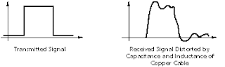 These effects are properties of transmission through metallic conductors, and become more pronounced as the conductor length increases. To compensate for distortion, signal power must be increased or the transmission rate decreased.
Special amplifier circuits are designed for transmitting direct (unmodulated) digital signals through cables. For the relatively short distances between components on a printed circuit board or along a computer backplane, the amplifiers are in simple IC chips that operate from standard +5v power. The normal output voltage from the amplifier for logic '1' is slightly higher than the minimum needed to pass the logic '1' threshold. Correspondingly for logic '0', it is slightly lower. The difference between the actual output voltage and the threshold value is referred to as the noise margin, and represents the amount of noise voltage that can be added to the signal without creating an error:

Subscribe to:
Comments (Atom)